
Heterogeneous Chiplets & Hybrid Bonding: The Modular Revolution Behind the Next Generation of Computing
Dive into the present

Intro
For decades, the entire semiconductor industry ran on a simple rule: shrink the transistor, shrink the chip, get more performance. Moore’s Law wasn’t just a prediction — it was a culture. Engineers believed that if you could just make everything smaller and put more on a single piece of silicon, the computer would keep getting better, faster, cheaper.
But physics has a sense of humor. As transistors reached atomic scales, shrinking became harder, hotter, and exponentially more expensive. The cost of building a modern chip factory now exceeds $20 billion. Yields are dropping. Heat is rising. The economics are breaking.
Meanwhile, AI demands more compute. Phones demand more battery efficiency. Cars demand more sensors, logic, and safety systems. And companies can no longer afford to build a giant monolithic chip that tries to do everything.
So the industry is pivoting — not by shrinking, but by breaking the chip apart.
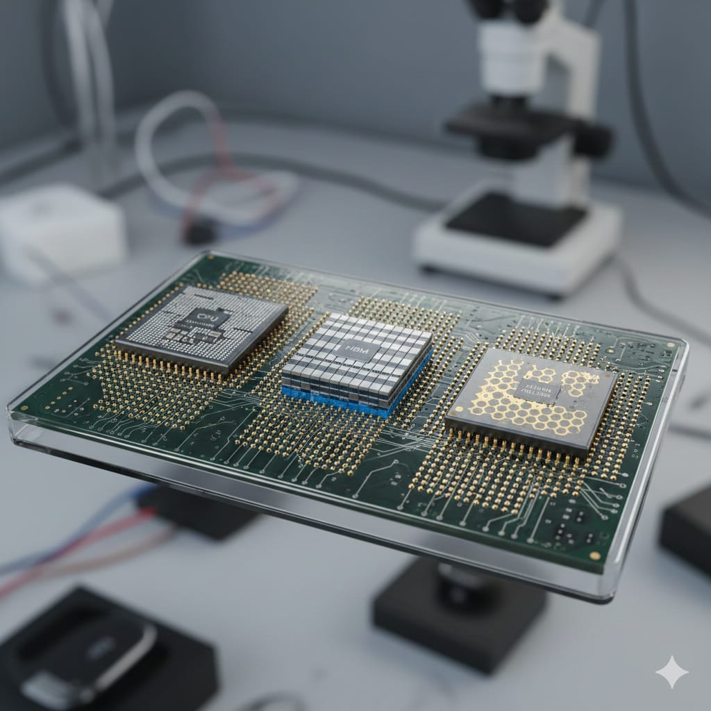
Welcome to the age of heterogeneous chiplets and hybrid bonding, a modular architecture that might define the next 20 years of computing. The idea is simple: instead of manufacturing one massive chip, you build many smaller specialized tiles — each on the best manufacturing node for its job — then fuse them together as if they were one.
The result?
- Higher performance.
- Lower cost.
- Better yields.
And a supply chain that behaves more like Lego blocks than fragile monolithic wafers.
This is the quiet revolution powering Apple Silicon, AMD’s EPYC processors, Tesla’s AI hardware, and soon… everything from VR headsets to data centers.
Why Chiplets Exist: The Death of the Monolithic Chip
A monolithic chip is a single continuous piece of silicon with billions of transistors etched onto it. It sounds simple, but the larger a chip is, the more likely it is to have a defect — and a single defect can ruin the entire die.
As chips grew bigger (to feed AI, graphics, and high-core-count CPUs), yields began to collapse.
Chiplets solve this by splitting the giant chip into smaller dies. If one dies fails, you only lose that small part, not the whole chip.
It’s the same reason we build ships out of sections instead of carving them out of one giant block of metal.
This isn’t just an engineering trick — it’s an economic miracle. AMD was one of the first to prove this with its Zen processors. By using chiplets, AMD achieved:
- over 40% cost reduction
- higher yields
- easier scalability
- better heat distribution
NVIDIA, Intel, Apple, and nearly every other major player followed.
But heterogeneous chiplets aren’t just about splitting the chip. They’re about mixing different types of silicon in the same package.
Heterogeneous = Mixing the Best of Everything
Different parts of a system run best on different manufacturing processes:
- CPUs like bleeding-edge 3nm logic
- GPUs need ultra-wide parallel units
- AI accelerators need dense compute arrays
- I/O controllers run fine on older, cheaper 14nm or 28nm
- Analog/RF circuits perform better on specialized nodes
- Memory needs a totally different manufacturing method
Trying to put all of that on one process is like asking one type of metal to behave like steel, copper, and aluminum simultaneously.
Heterogeneous chiplets solve this
Each chiplet is built on the process node that suits it best.
A modern chiplet CPU package may include:
- 3nm logic cores
- 5nm AI accelerators
- 7nm GPU units
- 28nm I/O
- 55nm analog
- stacked DRAM or SRAM on its own node
This is specialization at the silicon level, and it mirrors what biology has done for millions of years — different tissues for different jobs, arranged into one unified organism.
That “unified” part is the magic, and that’s where hybrid bonding enters the story.
Hybrid Bonding: The Superglue of the Future
You can’t just place chiplets next to each other and hope they cooperate. They need to talk — fast, efficiently, and with incredibly low latency.
Traditional packaging (like wire bonding or even microbumps) introduces limitations:
- slower data transfer
- more heat
- more energy consumption
- larger physical footprints
Hybrid bonding changes everything.
What Hybrid Bonding Is
Hybrid bonding is a technique where:
- Two chips are polished at the nanoscale so their surfaces are atomically flat
- They are aligned with microscopic precision
- Copper pads directly bond to copper pads
- The chips fuse on the molecular level, without bumps
Imagine two puzzle pieces clicking together, but at a scale where atoms align.
Compared to microbump technology(current way of prevaling chip tech), hybrid bonding gives:
- 10x more interconnect density
- higher bandwidth
- lower energy per bit
- dramatically reduced heat
- smaller spacing between chiplets
It’s the difference between two cities connected by a dirt road…and two cities connected by a hyperloop.
- This is why hybrid bonding is the secret sauce behind:
- Apple’s M1/M2/M3 “UltraFusion” architecture
- AMD’s 3D V-Cache
- HBM (High Bandwidth Memory) stacking
- AI accelerator packaging
- Next-gen server CPUs
- Military-grade low-power electronics
Hybrid bonding doesn’t just connect chiplets.
It makes them behave like one single chip.
How Chiplets + Hybrid Bonding Lower Costs
This is the part most people miss: chiplets aren’t just faster — they’re cheaper.
1. Higher Yields
Small dies fail less often. More usable dies per wafer = lower cost per chip.
2. Node Optimization
You only use expensive cutting-edge nodes for the parts that need it.Everything else runs on cheaper, mature processes.
3. Reusability
Chiplets are modular. A company can design a single I/O chiplet and reuse it across multiple processors for years.
4. Supply Chain Flexibility
Instead of relying on one fab for everything, companies can source different chiplets from different foundries.
This is a huge geopolitical advantage — especially for countries trying to reduce dependency on foreign fabs.
5. Faster Product Development
Updating a chip is as easy as swapping out or upgrading a module.
This is similar to software’s microservices revolution — except it’s happening in hardware.
The Real Game-Changer: AI
Here’s why the world cares so much:
- AI workloads are exploding.
- Models are getting bigger.
- Training requires exponential memory bandwidth and compute density.
- Monolithic chips simply cannot keep up.
Hybrid-bonded chiplets allow:
- stacked memory placed literally microns above compute tiles
- parallel compute chiplets stitched into massive arrays
- specialized AI blocks that can be swapped or scaled
- energy-efficient architectures with ultra-short interconnects
This is why NVIDIA, AMD, Intel, Tesla, and even OpenAI-backed startups are investing billions into chiplet research.
AI is becoming the biggest driver of semiconductor evolution since the rise of mobile computing.
The Future: Lego-Style Silicon
In the next decade, you’ll hear new terms:
- CSP (Chiplet Service Providers)
- Open Chiplet Marketplace
- UCIe 1.1 and beyond
- Chiplet interoperability standards
- Silicon IP marketplaces
Companies will be able to buy off-the-shelf chiplets the same way developers buy code libraries today. Imagine a world where designing a custom AI chip is as easy as assembling:
- an ARM CPU tile
- a specialized AI accelerator tile
- a GPU tile
- a memory tile
- a security tile
- a wireless tile
all bonded with hybrid connection layers into a single unit. Startups could enter markets previously reserved for billion-dollar giants.
This is how innovation accelerates.
Why This Revolution Is Inevitable
At its core, chiplets + hybrid bonding solve every major bottleneck we face today:
- performance
- power
- heat
- cost
- scalability
- supply chain fragility
- physical limits of monolithic dies
And it aligns perfectly with how the world is changing:
- AI needs massive compute
- mobile devices need extreme efficiency
- cloud providers need cheap scalability
- governments need manufacturing resilience
This isn’t a trend. It’s the new architecture of computing.
In the same way that microservices replaced monolithic software, chiplets are replacing monolithic silicon.
We’re not just shrinking chips anymore. We’re building them like ecosystems — modular, specialized, cooperative.
And hybrid bonding is the glue enabling that evolution.
A New Era of Silicon Biology
There’s something poetic about the direction this is all heading.
Nature itself solved complexity through modular, interconnected systems:
- organs work together
- tissues specialize
- cells communicate
- networks coordinate
Chiplets mirror this — small units of expertise bonded into one unified organism.
Silicon is getting closer to biology not by becoming alive, but by becoming modular. The next generation of computers won’t be monolithic machines. They will be multi-chiplet organisms, bonded with atomic precision, optimized for speed, density, and intelligence.
And somewhere in that architecture, the future of AI, edge computing, robotics, and quantum-scale systems will emerge.
We are entering a world where chips aren’t built — they are assembled, stacked, fused, and evolved.
The monolithic era is ending.
The modular era is beginning.
And hybrid bonding is the foundation on which the next century of computing will stand.
About the Creator
Sebastian De Lima
Dot…com?
Keep reading
More stories from Sebastian De Lima and writers in Futurism and other communities.
The Light-Speed AI Revolution: How Photonic Chips Could Make Smart Devices Faster and Cooler
Intro / Lede Imagine your phone running a powerful AI model without draining battery, or a tiny gadget that recognizes voice, images and learns on the fly — all while consuming a fraction of today’s power. That’s the real promise behind photonic AI chips: using light (photons) instead of electrons to do the heavy math. If industry and labs turn promise into products, the way we build and use AI could flip fast.
By Sebastian De Limaabout a month ago in Futurism
About Binding Prometheus
I want to start actively advocating on behalf of my own work, and the most valuable part of my canon is, without a doubt, Binding Prometheus, the play I have been working on since 2019 and only finished in 2023 as part of my MA. The play itself is an amalgamation of a million different inspirations. On one end, it evokes the Ancient Greek myth-play, deriving its own title from the earliest extant work of Western drama we have, Aeschylus’s Prometheus Bound. On the other end, it borrows significantly from the sci-fi bulwarks from over the years, namely Mary Shelley’s Frankenstein and Karel Capek’s Rossum’s Universal Robots. The play could be an episode of Black Mirror, I fear. I don’t know. I’ve only ever seen one episode of Black Mirror.
By Steven Christopher McKnight11 days ago in Futurism
The Ritual of Winter Challenge Winners
Welcome to the Winners Announcement for The Ritual of Winter challenge. This prompt focused on winter rituals and the meaning that settles into them over time. The top pieces stay grounded in ordinary acts and repeated routines, letting winter shape the work through pace, attention, and restraint.
By Vocal Curation Team3 days ago in Resources


Comments
There are no comments for this story
Be the first to respond and start the conversation.