
What's the best type
All you need to know about pn junctions
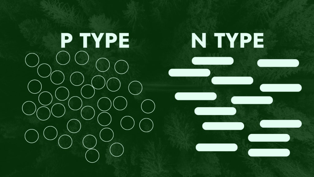
Table of content
Understanding PN Junctions
Formation of PN junction
Biasing in PN junction diode
Doping
Applications of PN junction diode
Conclusion
References
Understanding PN Junctions
A PN junction is a device formed when an N-type semiconductor material is joined with a P-type semiconductor material. The N-type material has an excess of free electrons, while the P-type material has an excess of holes. However, both materials are electrically neutral because the excess of free electrons and holes is balanced by the number of positive and negative ions, respectively.
When N-type material is joined to P-type material, the electrons in the N material diffuse across the junction into the P material and fill some of the holes, while the holes in the
P material diffuse across the junction into the N material and are filled by N material electrons. This process is called junction recombination and it reduces the number of free electrons and holes in the vicinity of the junction. Because there is a depletion, or lack of free electrons and holes in this area, it is known as the depletion region.
The diffusion of electrons and holes across the junction will continue until the magnitude of the electrostatic field is increased to the point where the electrons and holes no longer have enough energy to overcome it, and are repelled by the negative and positive ions respectively. At this point, equilibrium is established and, for all practical purposes, the movement of carriers across the junction ceases. For this reason, the electrostatic field created by the positive and negative ions in the depletion region is called a barrier.
PN junctions are important components in many electronic devices, including diodes, transistors, and solar cells. Understanding how they work can help us better understand how these devices function.
Formation of PN Junctions
The PN junction is created by the method of doping. Doping is the process of adding impurities to a semiconductor material to change its electrical properties. When a p-type semiconductor is doped with an n-type impurity, a PN junction is formed.
Doping can be achieved through several methods, including diffusion doping, ion implantation, and epitaxial growth. In diffusion doping, impurities are introduced into a semiconductor wafer by heating it in an atmosphere containing the desired impurity. In ion implantation, impurities are introduced into a semiconductor wafer by bombarding it with high-energy ions. In epitaxial growth, a thin layer of semiconductor material containing impurities is grown on top of a semiconductor wafer.
Once a PN junction has been formed through doping, it can be used in various electronic devices. For example, diodes are made by sandwiching a PN junction between two metal contacts. When a voltage is applied to these contacts, current flows through the diode in one direction but not in the other.
Biasing in PN junction diode
• In summary, the most important point to remember about the PN junction diode is its ability to offer very little resistance to current flow in the forward-bias direction but maximum resistance to current flow when reverse biased. A good way of illustrating this point is by plotting a graph of the applied voltage versus the measured current. The Figure below shows a plot of this voltage-current relationship (characteristic curve) for a typical PN junction diode.
Doping
• DOPING: process of adding impurities to pure semiconductors, to increase the number of free charges that can be moved by an external applied voltage.
• N-Type Semiconductor: An impurity is added to pure semiconductor to increases the number of free electrons, the doped semiconductor is NEGATIVE or N TYPE, and the impurity that is added is known as an N-type impurity.
• When a pentavalent (donor) impurity (Arsenic, antimony, bismuth, and phosphorous ) is added to germanium, it will form covalent bonds with the germanium atoms with one excess electron(majority carriers).
• Because these materials give or donate one electron to the doped material, they are also called DONOR impurities.
• P-Type Semiconductor: An impurity is added to pure semiconductor to reduce the number of free electrons, causing more holes(majority carries), creates a POSITIVE or P-TYPE semiconductor, and the impurity that was added to it is known as a P-type impurity
• Impurities of this type have only 3 valence electrons and are called TRIVALENT impurities. (Aluminum, indium, gallium, and boron)
• Because these materials accept 1 electron from the doped material, they are also called ACCEPTOR impurities.
Applications of PN Junctions
PN junctions are elementary “building blocks” of semiconductor electronic devices such as diodes, transistors, solar cells, light-emitting diodes (LEDs), and integrated circuits; they are the active sites where the electronic action of the device takes place.
Diodes are one of the most common applications of PN junctions. A diode is an electronic device that allows current to flow in one direction but not in the other. Diodes are used in many electronic circuits to control the flow of current or to convert alternating current (AC) into direct current (DC).
Transistors are another common application of PN junctions. A transistor is an electronic device that can amplify or switch electronic signals. Transistors are used in many electronic circuits to amplify weak signals or to control other electronic devices.
Solar cells are another application of PN junctions. A solar cell is an electronic device that converts sunlight into electricity. Solar cells are made from semiconductor materials that contain PN junctions. When sunlight strikes a solar cell, it generates an electric current that can be used to power electronic devices.
Light-emitting diodes (LEDs) are another application of PN junctions. An LED is an electronic device that emits light when an electric current passes through it. LEDs are made from semiconductor materials that contain PN junctions. When an electric current passes through an LED, it generates light that can be used for illumination or for displaying information.
Integrated circuits (ICs) are another application of PN junctions. An IC is an electronic device that contains many transistors and other components on a single chip of semiconductor material. ICs are used in many electronic devices to perform complex functions such as processing data or controlling other electronic devices.
Conclusion
PN junctions are important components in many electronic devices such as diodes, transistors, solar cells, LEDs, and ICs. Understanding how they work can help us better understand how these devices function.
References:
• [Wikipedia - PN Junction]
About the Creator
Keep reading
More stories from writers in Education and other communities.
Innovation and Adaptability in Action: How to Thrive in a Fast-Changing World
The modern world changes fast. New tools, new ideas, and new challenges appear every day. People and organizations must respond with speed and purpose. This is why innovation and adaptability matter more than ever. These skills help individuals, teams, and businesses stay strong during change. They support growth, learning, and long-term success. When change feels constant, the right mindset can turn risk into opportunity. Innovation and adaptability are not abstract ideas. They are daily actions. They guide how we solve problems, learn new skills, and adjust plans. They help us move forward when old ways no longer work. In a world shaped by technology, climate issues, and social shifts, these qualities are essential.
By Brian Ferdinand4 days ago in Education
Autonomy Is The Real Privilege
Good morning, freedom-seekers! Today we’re gonna be looking at autonomy. A strange word, I know; one many would probably look at blankly and run away from on sight. We’re gonna figure out what it actually means, consider how it’s achieved, and decipher just how deeply most of us are tangled up in dependence without realising it.
By That ‘Freedom’ Guy5 days ago in Humans
Book Review: "The Queen" by Andrew Morton
You're probably wondering why on earth I would read this book. It was free and it was a fair length. That was basically it at first. But another reason is because I enjoyed the show The Crown and so, it only makes sense to read a book that goes through separating facts from fictions - and to be fair, there aren't a lot of fictions about the show it seems. From the birth of the little princess and the way in which her father was reluctantly to become the king, all the way to meeting and marrying the veteran prince, Duke of Edinburgh and even down to the death of her father, queendom and beyond, this book actually gives us a lot about a woman who basically embodied the greatness and modernisation of the British 20th Century.
By Annie Kapur7 days ago in Geeks


Comments (1)
It was very educative,it helped in my exams.😭