
The Complete Guides of PCB Assembly Services: The Process and How Works
PCB assembly process involves DFA, SMT and through-hole components placement, testing, and final inspection.
What is PCB assembly service?
The PCB assembly services comprise a vital step in the electronics manufacturing process, where cutting-edge technology is utilized to mount electrical components onto printed circuit boards. This operation is also referred to as printed wiring assembly, circuit card assembly, and electronics assembly.
Efficient and precise PCB assembly services are crucial for the development of the electronics industry. Additionally, they offer cost-saving advantages by reducing manufacturer labor expenses.
Printed Circuit Boards Assembly (PCBA) Process
Electronics play a crucial role in our everyday routines, encompassing everything from our mobile devices to our vehicles, which are all powered by electronic components. At the core of these advanced technologies lies the printed circuit board, commonly referred to as a PCB.
These are commonly known as printed circuit boards, typically seen as small green chips covered in lines and copper parts at the core of disassembled electronic devices. They are typically constructed with fiberglass, copper lines, and other metal parts, and are held together by epoxy and insulated by a solder mask, which gives them their signature green hue.
Although often overlooked, the components solidly stuck on circuit boards serve a vital purpose and should not be dismissed as mere decorations. In order for a circuit board to function properly, it must have components mounted on it. This process is known as PCB assembly or PCBA for short. The copper traces on the bare board act as electrical pathways, connecting the various connectors and components and allowing the board to perform its intended functions. These functions can range from simple to complex, and remarkably, PCBs can be smaller than a thumbnail in size.
Learn more about how these devices are manufactured. The PCB assembly process involves both automated and manual steps. During each step, board manufacturers have a variety of options to choose from, including both manual and automated methods. To gain an understanding of the complete PCBA process, we have outlined each step in detail below.
PCB Design Basics
The initial stage of the PCBA process involves the fundamental element of the PCB: the base. Comprised of multiple layers, each one serves a crucial function in determining the overall functionality of the end product. These layers are interspersed with one another and have various responsibilities.
• Substrate: This is the base material of a PCB. It gives the PCB its rigidity.
• Copper: A thin layer of conductive copper foil is added to each functional side of the PCB — on one side if it's a single-sided PCB, and on both sides if it's a double-sided PCB. This is the layer of copper traces.
• Solder mask: The copper layer is topped with a solder mask in a distinct green color, which serves to insulate copper traces and prevent accidental contact with other conductive materials, avoiding any potential shorts. Solder is applied through holes in the solder mask to attach components to the PCB, ensuring everything stays in its proper place. The application of solder mask is crucial for a seamless PCBA manufacturing process, as it prevents solder from being applied to unwanted areas, preventing shorts.
• Silkscreen: The final layer of a PCB board is a white silkscreen that adds labels in the form of characters and symbols, indicating the function of each component.
Parts and materials used in PCBs typically remain consistent, except for the substrate which varies depending on the desired characteristics such as cost and flexibility, as determined by the designer.
The three primary PCB types include:
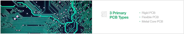
• Rigid PCB: Rigid PCB bases, which make up the majority of PCBAs, are typically made from a solid core that provides both rigidity and thickness. These inflexible bases are commonly constructed with materials such as fiberglass, known as "FR4", while less expensive options may use epoxies or phenolics, which are not as durable.
• Flexible PCB: Flexible PCBs are known for their increased pliability compared to rigid counterparts. They are typically made with a bendable, high-temperature plastic material such as Kapton.
• Metal Core PCB: These boards are a viable alternative to traditional FR4 boards. With a metal core, these boards are able to efficiently distribute heat and safeguard heat-sensitive board components. This results in better heat dissipation.

There are two types of mounting technologies are prevailing in the modern PCBA industry:
Surface Mount Technology: Sensitive components, some very small, such as resistors or diodes are placed automatically onto the surface of board. This is called SMD assembly, for surface mount device. Surface mount technology can be applied on small size components and integrated circuits (ICs). For example, PCBCart is capable of mounting package with min. size 01005, which is even smaller than the size of a pencil point.
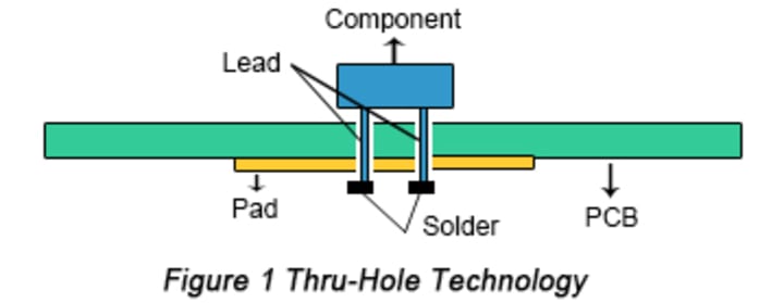
Thru-Hole Technology: works well on components with leads or wires that have to be mounted on board by plugging them through holes on board. The extra lead part has to be soldered on the other side of the board. This technology is applied on PCB assemblies containing large components such as capacitors, coils to be assembled.
The assembly process for THT and SMT differs due to their distinctions. This article will cover additional considerations for materials and design in the PCB assembly process, specifically for THT, SMT, and mixed technologies.
Before the Assembly Process
Before initiating the PCBA process, it is necessary to complete a few preparatory steps. These steps allow PCB manufacturers to evaluate the functionality of a PCB design, and typically involve a DFM check.
In order to begin the PCB assembly process, it is important for companies to provide the PCB design file, design notes, and specific requirements. This allows the assembly company to thoroughly review the file for any potential issues that could impact the functionality or manufacturability of the PCB. This is commonly referred to as a Design for Manufacturability check, or DFM check for short.

The DFM check analyzes all PCB design specifications for any missing, redundant, or problematic features that may greatly impact the final project's functionality. A common flaw to be mindful of is insufficient spacing between components, which can lead to shorts and other malfunctions.
Our DFM checks are a crucial step in the manufacturing process, helping to prevent costly issues and reduce the number of scrapped boards. As part of our dedication to providing quality at an affordable price, every PCBCart project order includes FREE DFM and DFA checks. These checks are powered by the automatic system Valor DFM/DFA, known for its quick speeds and precise results.
Actual PCBA process steps.
Step 1: Solder Paste Stenciling
During the PCB assembly, a solder paste is applied to the board by using a stencil made of stainless steel. This is similar to the process of screen-printing a shirt, but instead of a mask, the stencil is placed on top of the PCB. This technique enables assemblers to accurately apply solder paste to specific areas of the board where components will be placed in the final product.
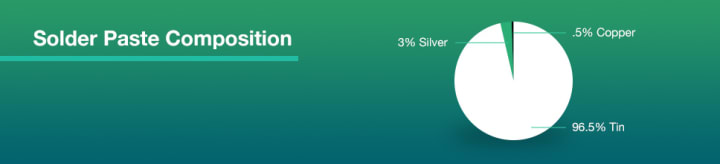
The solder paste is composed of 96.5% tin, 3% silver, and 0.5% copper, and is made up of tiny metal balls. It must be accurately applied to the circuit board using a flux, which aids in the melting and bonding process. The paste itself has a grey appearance and should be applied with precision in specific locations and quantities.
A mechanical fixture is used in a professional PCBA line to securely hold the PCB and solder stencil. Once in place, an applicator precisely applies solder paste to designated areas. The machine then evenly distributes the paste across the stencil, ensuring complete coverage. Once the stencil is removed, the solder paste remains in the designated locations.
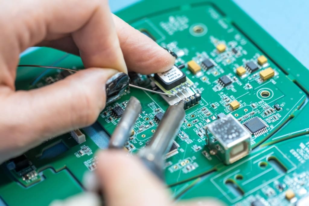
Step 2: Pick and Place
Following the application of solder paste to the PCB board, the PCBA process proceeds to the pick and place machine, where a robotic device precisely positions surface mount components, also known as SMDs, on the prepared board. SMDs are the most commonly used non-connector components on modern PCBs, and are then soldered onto the surface of the board in the following step of the PCBA process.
Originally, assembling components was a manual task using tweezers. However, advancements in PCB manufacturing have allowed for automated pick and place processes. This change is due to the precision and consistency of machines, which outperform humans in this task. Despite being able to work quickly, humans often experience fatigue and eyestrain after a few hours of handling such delicate components. In contrast, machines can work continuously without these limitations.

The process begins with the device picking up a PCB board using a vacuum grip and transferring it to the pick and place station. Once at the station, the robot aligns and applies the SMTs to the PCB surface according to preprogrammed coordinates, on top of the soldering paste.
Step 3: Reflow Soldering
To ensure successful PCB assembly, it is crucial to maintain the position of both the solder paste and surface mount components until the paste solidifies and effectively bonds the components to the board. This is accomplished through the essential process of "reflow".
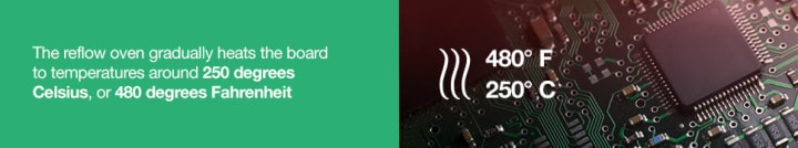
Upon completion of the pick and place process, the PCB board is transferred to a conveyor belt. This belt guides the board through a reflow oven, which is comparable to a commercial pizza oven, gradually heating it using a sequence of heaters. The board reaches temperatures as high as approximately 250 degrees Celsius or 480 degrees Fahrenheit, resulting in the melting of solder in the solder paste.
As the solder is melted, the PCB progresses through the oven and encounters a sequence of cooler heaters. This controlled cooling process causes the molten solder to solidify, resulting in reliable and permanent solder joints to connect the SMDs to the PCB.
For optimal results, it is important to carefully consider the reflow process for PCBAs, particularly for two-sided PCB assembly. To ensure proper placement and reflow, each side of the board must be stenciled and processed individually. The first step is to stencil and reflow the side with fewer and smaller components, followed by the second side.
Step 4: Inspection and Quality Control
Upon completion of the reflow process and soldering of surface mount components, the assembled board must undergo functional testing. Movement during the reflow process may lead to subpar connection quality or a lack of connection, as well as the possibility of shorts caused by misplaced components connecting unintended portions of the circuit. It is vital to test for functionality to avoid these potential issues.

Possible inspection methods for identifying errors and misalignments include various techniques. Among the most frequently used techniques are those commonly referred to as inspection methods.:
• Manual Checks: While automated and smart manufacturing are growing in popularity, manual checks remain a crucial step in the PCB assembly process. For smaller batches, designers can ensure the quality of a PCB after the reflow process through an in-person visual inspection. However, as the number of inspected boards increases, this method becomes less practical and accurate due to optical fatigue potentially leading to less accurate inspections.
• Automatic Optical Inspection: The merchant recommends utilizing automatic optical inspection for larger batches of PCBAs. This method, also known as an AOI machine, employs multiple high-powered cameras to visually inspect PCBs. The cameras are strategically positioned to view solder connections from various angles, enabling the AOI to identify weaker solder joints based on light reflections. With its high processing speed, the AOI is capable of examining a large volume of PCBs in a short period of time.
• X-ray Inspection:One alternative for inspection is utilizing X-rays, which is typically reserved for intricate or multi-layered PCBs. It permits observation of inner layers and detection of any possible concealed issues.
If a board malfunctions, the PCBA company's standards will determine whether it is cleared and reworked or scrapped.
In order to ensure proper functionality, the next step after an inspection is to conduct a thorough testing of the part. This includes a quality check of the PCB connections. In the case of boards that need programming or calibration, additional steps are necessary to ensure their proper functioning.
Inspections are often conducted after the reflow process to detect any potential issues. These routine assessments are crucial in identifying and addressing errors promptly, resulting in time and resource savings for both the manufacturer and designer.
Step 5: Through-Hole Component Insertion
The PCBA board may contain additional components besides standard SMDs, depending on its type. Such components may include plated through-hole (PTH) components.
A plated through-hole allows for the transfer of signals from one side of the PCB to the other. Soldering paste is ineffective in this situation, as it will simply pass through the hole without adhering.
To complete the PCB assembly, PTH components require a specific soldering method rather than soldering paste. This ensures a successful and efficient process.:
• Manual Soldering: The process of manual through-hole insertion is quite simple. A single person is usually responsible for inserting one component at a designated PTH station. This person then hands off the board to the next station, where another individual inserts a different component. This cycle repeats for each PTH that needs to be outfitted, making the process longer depending on the number of PTH components that need to be inserted during a single PCBA cycle. Although many companies try to avoid using PTH components in their designs, they are still commonly used in PCB designs.
• Wave Soldering: Wave soldering is the automated version of manual soldering, but involves a very different process. Once the PTH component is put in place, the board is put on yet another conveyor belt. This time, the conveyor belt runs through a specialized oven where a wave of molten solder washes over the bottom of the board. This solders all of the pins on the bottom of the board at once.This kind of soldering is nearly impossible for double-sided PCBs, as soldering the entire PCB side would render any delicate electronic components useless.
Upon completion of the soldering process, the PCB can proceed to final inspection. It may also revisit previous steps in the event that additional parts need to be added or another side needs to be assembled.
Step 6: Final Inspection and Functional Test
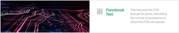
After the soldering step of the PCBA process is complete, the PCB undergoes final inspection to determine its functionality. This testing procedure, known as a "functional test", replicates normal operational conditions to thoroughly evaluate the PCB's performance. Power and simulated signals are run through the PCB during this test, with testers closely monitoring its electrical characteristics.
The PCB may be recycled or scrapped in accordance with company standards if any of its characteristics, such as voltage, current, or signal output, exhibit excessive fluctuations or exceed a predetermined range during testing.
The process of PCB assembly is incomplete without thorough testing, which plays a critical role in determining its success or failure. That's why it's crucial to conduct continuous testing and inspection throughout the entire process.
After PCBA
When completing the PCB assembly process, it is important to note that soldering paste may leave behind flux and human handling can transfer oils and dirt onto the PCB surface. These factors can lead to a less than ideal appearance and also pose practical concerns.
Washing the product after completing the soldering process is crucial due to the development of a sticky and smelly residue on PCBs over time. This residue is not only acidic and harmful to solder joints, but it can also negatively impact customer satisfaction when new PCB shipments are covered in residue and fingerprints. Follow this important step to maintain the quality of your product.
A high-pressure washing apparatus made of stainless steel and using deionized water is the most effective method for removing residue from PCBs. PCBs can be safely washed in deionized water without any risk to the device. This is due to the fact that it is the ions found in regular water that cause damage to circuits, not the water itself. As a result, deionized water is harmless to PCBs during the wash cycle.
Following thorough cleaning, utilizing a rapid drying process involving compressed air efficiently prepares the PCBs for packaging and transportation.
Differences between PCBAs: THT Assembly, SMT Assembly and Mixed Technology
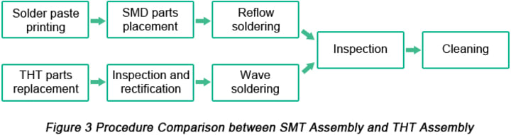
Thru-Hole Technology (THT) Assembly Process
The thru-hole mounting process, a traditional method for PCB assembly, relies on a combination of manual and automatic procedures to complete..
• Step 1: The placement of components is a crucial step in the PCB manufacturing process, requiring skilled engineers to manually arrange them according to the client's design specifications. In order to maintain high quality standards, the engineers must adhere to regulations and operation standards for thru-hole mounting, such as ensuring proper polarity and orientation of components and wearing anti-static wristbands when handling sensitive components like ICs. These meticulous measures guarantee a top-notch end product that is compatible with industry standards..
• Step 2: Once component placement is finished, the board is put into a corresponding transport frame for automatic inspection to ensure accurate placement. If any issues are found, they can be rectified immediately before the soldering process begins. This step is crucial for ensuring high-quality results in the PCBA process..
• Step 3: In the process of wave soldering, the circuit board is slowly moved over a high temperature liquid solder so that THT components can be accurately and securely attached. This method allows for successful connections with all leads and wires.
Mixed Technology
As modern science and technology advances, electronic products are becoming more intricate and requiring smaller, integrated PCB boards. This makes it nearly impossible for single-component PCBAs to be utilized.
Consider incorporating both thru-hole technology and surface mount technology when assembling a board. It's important to carefully arrange the sequence of components to ensure successful soldering, as this process can be affected by many factors.
PCBA with application of mixed technologies should be carried out in the following situations:
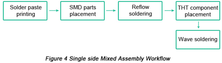
• Single Side Mixed Assembly: The manufacturing procedure for this product includes mixed assembly on one side. However, for small quantities of through-hole components, hand soldering can be used instead of wave soldering.
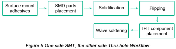
• One Side SMT One Side THT: Please note that using adhesives during the PCB assembly process is not recommended as it can increase the total cost of PCBA and potentially cause soldering issues.
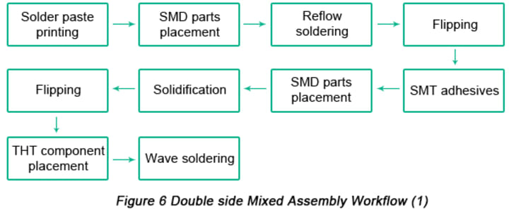
• Double Side Mixed Assembly:When it comes to double side mixed assembly methods, there are two options available: applying adhesives during PCBA or not. Unfortunately, the use of adhesives can significantly raise the cost of PCB assembly. Additionally, this process will require the PCB to be heated three times, which can result in lower efficiency.
In regards to the previously mentioned mixed assembly procedures, it can be determined that hand soldering is suitable for PCB assembly with a large number of components on both sides, particularly SMD components. As such, when faced with a scenario where only a few THT components are needed, wave soldering is recommended.
The complex and technical process of PCB assembly requires careful consideration of numerous elements. Any small modifications can greatly impact cost and product quality. This article focuses on the standard procedures and technologies involved in the PCBA process. The practical manufacturing process is heavily influenced by design files and customer requirements.
About the Creator
Keep reading
More stories from china inspection service and writers in 01 and other communities.
The Compleate Guide of Connecting Raspberry Pi through SSH
How to SSH into a Raspberry Pi This article is designed to educate you on the process of SSHing into a Raspberry Pi and resolving any common connection problems. Additionally, it will introduce a different method for accessing your Pi through SSH with the help of Tailscale.
By china inspection service12 months ago in 01
Why People Are Drawn to Replica Watches: A Look at Culture, Craft, and Perception
In the world of watches, value is often tied to rarity, heritage, and craftsmanship. Luxury brands inspire admiration not only because of their mechanical precision but also because they represent decades—sometimes centuries—of design history. Yet alongside these celebrated originals exists another category that generates constant conversation: replica watches.
By charliesamuel4 days ago in 01


Comments
There are no comments for this story
Be the first to respond and start the conversation.