
Silicon Wafer Market: Global Semiconductor Ecosystem, Investment Trends & Market Forecast
Demand for high-purity and large-diameter wafers supports market growth.

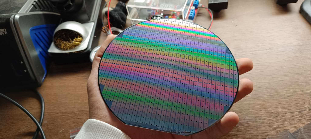
According to IMARC Group's latest research publication, global silicon wafer market size reached USD 27.8 Billion in 2025. Looking forward, IMARC Group expects the market to reach USD 46.71 Billion by 2034, exhibiting a growth rate (CAGR) of 5.64% during 2026-2034.
How AI is Reshaping the Future of Silicon Wafer Market
- Predictive Quality Control and Defect Detection: Machine learning algorithms analyze high-resolution wafer images in real-time, identifying microscopic surface defects, contamination, and pattern anomalies with exceptional precision.
- Advanced Process Control and Virtual Metrology: AI-driven systems continuously monitor and adjust manufacturing parameters during crystal growth, wafer slicing, and polishing operations based on real-time sensor data.
- Automated Production Optimization and Energy Management: Artificial intelligence analyzes vast datasets from production lines to identify efficiency patterns and optimize resource allocation across wafer manufacturing facilities.

Silicon Wafer Industry Overview:
The semiconductor industry's explosive growth is driving unprecedented demand for silicon wafers, fueled by government initiatives and massive infrastructure investments worldwide. The U.S. CHIPS and Science Act has allocated over $39 billion in direct funding to strengthen domestic semiconductor manufacturing, with GlobalWafers receiving $406 million to establish America's first high-volume 300mm wafer production facilities in Texas and Missouri, creating approximately 2,580 jobs.
Silicon Wafer Market Trends & Drivers:
The artificial intelligence revolution and data center expansion are reshaping silicon wafer demand across the technology landscape. AI chip manufacturing for training large language models and inference workloads requires leading-edge process nodes below 5nm, driving demand for high-quality 300mm wafers with exceptional flatness and purity specifications.
Electric vehicle adoption and renewable energy transitions are creating substantial opportunities for specialized wafer products beyond traditional computing applications. The EV market requires power semiconductors fabricated on silicon carbide wafers, which offer superior performance in high-voltage battery management and charging systems compared to conventional silicon.
Miniaturization demands and advanced packaging innovations are pushing wafer technology toward larger diameters and enhanced material properties. The transition from 200mm to 300mm wafers enables chipmakers to produce more dies per wafer, improving manufacturing economics through better material utilization and reduced per-unit costs.
Leading Companies Operating in the Global Silicon Wafer Industry:
- GlobalWafers Singapore Pte. Ltd.
- Okmetic Oy
- Shanghai Simgui Technology Co. Ltd.
- Shin-Etsu Chemical Co., Ltd.
- Silicon Materials, Inc.
- Siltronic AG
- SK Siltron Co., Ltd.
- Sumco Corporation
- Tokuyama Corporation
- Virginia Semiconductor, Inc.
- Wafer Works Corporation
Silicon Wafer Market Report Segmentation:
By Wafer Size:
- 300mm
- 200mm
- 150mm
- Others
300mm represents the largest segment, accounting for around 68.3% of the market, as larger wafers enable manufacturers to produce more chips per wafer, resulting in improved cost-efficiency and higher yields.
By Type:
- P-type
- N-type
P-type dominates the market with approximately 57.1% share, serving as the primary substrate for integrated circuit manufacturing across electronic devices.
By Application:
- Integrated Circuits
- Solar Cells
- Others
Integrated circuits lead the market with around 50.1% share due to their central role in powering modern electronics from smartphones to data centers.
By End Use:
- Solar
- Consumer Electronics
- Telecommunications
- Automotive
- Industrial
- Others
Solar leads the market with approximately 42.1% share, driven by global renewable energy adoption and photovoltaic cell production requirements.
Regional Insights:
- North America (United States, Canada)
- Asia Pacific (China, Japan, India, South Korea, Australia, Indonesia, Others)
- Europe (Germany, France, United Kingdom, Italy, Spain, Russia, Others)
- Latin America (Brazil, Mexico, Others)
- Middle East and Africa
Asia Pacific dominates the silicon wafer market with 68.5% share due to concentrated semiconductor manufacturing capacity, established supply chains, and favorable government policies supporting technology innovation.
Recent News and Developments in Silicon Wafer Market
- December 2024: GlobalWafers received $406 million in CHIPS Act funding to support construction of 300mm silicon wafer manufacturing facilities in Texas and Missouri, representing total capital expenditures of approximately $4 billion.
- November 2024: TSMC finalized its $6.6 billion direct funding agreement under the CHIPS Incentives Program to expand advanced semiconductor manufacturing in Arizona.
Note: If you require specific details, data, or insights that are not currently included in the scope of this report, we are happy to accommodate your request. As part of our customization service, we will gather and provide the additional information you need, tailored to your specific requirements. Please let us know your exact needs, and we will ensure the report is updated accordingly to meet your expectations.
About the Creator
sujeet. imarcgroup
With 2 years of hands-on experience at IMARC Group, I have conducted in-depth market research and analysis across diverse industries including technology, healthcare, agriculture, and consumer goods.
Keep reading
More stories from sujeet. imarcgroup and writers in Futurism and other communities.
Supply Chain Finance Market: Blockchain & Smart Contracts, Transparency Enhancement & Market Forecast
According to IMARC Group's latest research publication, global supply chain finance market size reached USD 8.1 Billion in 2025. Looking forward, IMARC Group expects the market to reach USD 15.8 Billion by 2034, exhibiting a growth rate (CAGR) of 7.68% during 2026-2034.
By sujeet. imarcgroupabout 8 hours ago in Futurism
Australia Oral Care Market: Preventive Hygiene, Consumer Awareness & Product Innovation
According to IMARC Group, the Australia oral care market reached a value of USD 1.1 Billion in 2025 and is projected to expand to USD 2.3 Billion by 2034, exhibiting a compound annual growth rate (CAGR) of 7.74% during 2026–2034. This strong growth trajectory highlights a structural shift in how consumers perceive oral hygiene—from a basic daily routine to a core component of preventive healthcare and overall wellness. Rising awareness of the link between oral health and systemic conditions such as cardiovascular disease and diabetes is reshaping purchasing behavior, while innovation in products and delivery formats is broadening market appeal. As consumer expectations evolve toward efficacy, convenience and sustainability, oral care has become a dynamic and innovation-driven segment of the broader personal care market across Australia.
By Shrestha Roy2 days ago in Futurism


Comments
There are no comments for this story
Be the first to respond and start the conversation.