
Researchers use light and crystals to create new materials on demand.
This recent advancement makes use of a phenomena known as plasmonic heating, which permits more accurate crystal formation.

One day, it may be possible to "draw" rather than "grow" crystals for use in a wide range of applications, including lasers, LEDs, and the semiconductors used in sensors in astronomical instruments, which would result in improved performance and reduced prices.
A group from Michigan State University, led by Elad Harel, has heated a gold nanoparticle with a laser, causing crystal formation in a lead halide perovskite solution. So, theoretically, it is conceivable to precisely 'draw' the crystals where they need to be in an electronic system by manipulating the gold nanoparticle, once more with the use of lasers.
Traditional methods for creating crystals for electronics include planting a crystal "seed" and then watching it grow, or vapour diffusion, in which the crystal precipitates out of a solution. These techniques, however, are imprecise and result in crystals that grow very randomly and aren't always in the proper place, shape, or size.
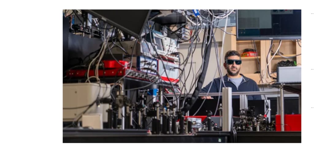
"In a device, one may need a very small quantity of crystalline material placed at very specific locations," Harel stated to Space.com.
By employing a process called "plasmonic heating," Harel's novel method restores some degree of control over crystal formation. In lab tests, Harel's group aimed a 660 nm laser at a gold nanoparticle in a reaction chamber that contained the lead halide perovskite precursor solution over a borosilicate glass substrate that the crystal would be "drawn" onto.
The gold nanoparticle is minuscule, measuring less than a thousandth of a human hair's width. The entire process must therefore be incredibly accurate and observable in real time through the use of high-speed microscopes with frame rates of sub-millisecond intervals.
"The reason we use gold nanoparticles is because they act as small heaters," Harel stated. "When a laser irradiates the particle at the right frequency, it causes the electrons in the gold to oscillate, which generates heat." Plasmonic heating is what causes the precursor solution to crystallise in the precise places that Harel's group wants it to.
Although they perform well in solar cells and LEDs, lead halide perovskite crystals are not the only kind of crystal utilised in electronics. For instance, arsenic-doped silicon crystals are used in the semiconductors of the James Webb Space Telescope's Mid-Infrared Instrument (MIRI). Harel thinks that this plasmonic heating technique can be applied to other similar crystals, but it works for lead halide perovskites specifically because they have some very peculiar features.
"What's special about these perovskites is that as the temperature increases the solubility decreases, which induces crystallisation," he stated. "Most materials do not exhibit this retrograde solubility property; typically as the temperature increases, the solubility increases."
But the jiggling, stimulated electrons might hold the key to a solution. According to Harel, the electrons might theoretically directly contribute to the chemistry of crystal formation in addition to generating heat, hence promoting crystal formation. "We do need to do more work to generalise this concept to other materials, but we believe it will work," he stated.
The benefits of more accurate, quicker, and less expensive crystal formation are obvious. Touchscreens, smoke detectors, solar panels, medical imaging equipment, and the majority of optoelectronics and photodetectors in general all employ crystals.
"This is a very simple method using low-cost lasers," Harel stated. "It also saves enormously on the cost of fabrication since the crystal could be placed exactly where and when it is needed."
Because of the significance of crystals for astronomical sensing, the process of drawing them may even lead to the future deployment of less expensive devices on space missions.
The next stage is to try to "draw" more complex crystal patterns using several lasers at different wavelengths. After that, they will be tested in actual devices to see if they actually provide a higher quality of performance at a lower cost. "This is something we're working on right now," Harel replied.
About the Creator
Keep reading
More stories from Francis Dami and writers in Futurism and other communities.
A new telescope photograph shows the interstellar comet 3I/ATLAS blasting a jet towards the sun.
As our nearest star warms up a portion of the comet's surface, 3I/ATLAS is launching a jet of material in the direction of the sun. The composite image displays a white light, which is the comet's atmosphere or coma, and the nucleus, or frozen, rocky centre core, of 3I/ATLAS as a big, black dot. The purple-marked jet is blazing out in the direction of the sun, which is also how comets in the solar system often behave.
By Francis Dami5 months ago in Futurism
Kids Digital Advertising Market to hit USD 25.9 Billion By 2033
The Global Kids Digital Advertising Market is projected to reach approximately USD 25.9 Billion by 2033, rising from USD 3.4 Billion in 2023, and is expected to expand at a CAGR of 22.5% during the forecast period from 2024 to 2033. This growth is driven by the increasing digital consumption among children, the growing influence of social media, and the rising importance of targeted, interactive advertising methods. With the increasing use of smartphones, tablets, and other digital devices among kids, advertisers are increasingly focusing on creating engaging, child-friendly content that can capture the attention of younger audiences.
By Roberto Crum4 days ago in Futurism
Artemis II: Nasa targets early April for Moon mission
The mission represents a crucial milestone in NASA’s broader Artemis program, which aims to return humans to the lunar surface and establish a long-term presence on the Moon. If successful, Artemis II will pave the way for future missions that could eventually support lunar bases and deeper exploration into the solar system. Artemis II will be the first crewed flight of the powerful Orion spacecraft launched aboard the massive Space Launch System rocket. The spacecraft will carry four astronauts on a journey that will take them thousands of kilometers beyond the Moon before returning safely to Earth. The mission follows the success of Artemis I, which flew in late 2022 and successfully tested the Orion spacecraft in deep space without astronauts on board. That mission orbited the Moon and returned valuable data about the spacecraft’s performance, heat shield durability, and onboard systems. According to NASA officials, Artemis II will take astronauts on a roughly 10-day journey. During the mission, the Orion spacecraft will perform a flyby of the Moon, traveling farther from Earth than any human mission has gone before. The astronauts will also test key navigation systems, life-support technology, and communication equipment needed for long-duration space travel. The crew selected for the historic mission includes commander Reid Wiseman, pilot Victor Glover, mission specialist Christina Koch, and Canadian astronaut Jeremy Hansen. Together, they will represent a new era of international cooperation in space exploration. Christina Koch’s participation is particularly significant, as she will become the first woman to travel to the Moon. Meanwhile, Jeremy Hansen will be the first Canadian astronaut to take part in a lunar mission, highlighting the role of international partnerships in NASA’s long-term exploration strategy. The Artemis program itself is part of a broader effort to establish sustainable human exploration beyond Earth. Unlike the earlier Apollo missions, which focused on short lunar visits, the Artemis program aims to build infrastructure that will support repeated missions and long-term scientific research. Future plans include the construction of the Lunar Gateway, a small space station that will orbit the Moon and serve as a staging point for missions to the lunar surface. From there, astronauts could travel down to the Moon using specialized landers designed for repeated use. NASA officials say the Artemis program will also help prepare astronauts for future missions to Mars. By testing deep-space systems near the Moon, engineers and scientists can learn valuable lessons about life-support systems, radiation protection, and long-duration spaceflight. Despite the excitement surrounding Artemis II, the mission has faced multiple delays as engineers worked to ensure the safety of both the spacecraft and the launch system. Issues related to hardware testing, battery components, and environmental control systems required additional time for inspection and redesign. NASA administrators have emphasized that safety remains the agency’s top priority. Crewed missions beyond low Earth orbit carry significant risks, and officials have insisted that all systems must be thoroughly tested before astronauts are launched into deep space. The early April target represents a tentative launch window rather than a fixed date. Weather conditions, final technical checks, and launch readiness reviews will ultimately determine the exact day when the rocket lifts off from Kennedy Space Center. If the mission proceeds as planned, Artemis II will become the first crewed lunar flyby mission since Apollo 17 in 1972. That historic mission marked the end of the Apollo era, after which human exploration of the Moon paused for decades. Now, with Artemis II approaching launch, NASA is preparing to usher in a new chapter of lunar exploration. The mission is expected to capture global attention as astronauts once again venture into deep space, retracing a path last traveled by the Apollo generation. For space enthusiasts, scientists, and engineers around the world, the upcoming mission represents more than just a technological achievement. It symbolizes humanity’s renewed determination to explore beyond Earth and expand our understanding of the universe. If Artemis II succeeds, it will not only demonstrate the readiness of NASA’s next-generation spacecraft but also bring humanity one step closer to returning astronauts to the lunar surface for the first time in the 21st century.
By Fiaz Ahmed a day ago in Futurism


Comments
There are no comments for this story
Be the first to respond and start the conversation.